(Last Mod: 27 November 2010 21:56:32 )
Linear feedback shift registers provide pseudorandom bit sequences for a variety of purposes, ranging from simple (and rather poor) random number generators to chip sequence generators for direct sequence spread spectrum communication systems.
Linear feedback shift registers are a direct embodiment of finite field arithmetic. To be more specific, they directly perform polynomial arithmetic in a GF(2n) extension field. The most basic such shift register does nothing more than update the presently represented polynomial by multiplying it by the formal variable and reducing the result modulo-M where M is a primitive polynomial.
In addition to being based on highly rigorous mathematic principles, which permit highly detailed analyses of the behavior of systems utilizing them, the use of linear feedback shift registers possess another important attribute - they are easy to implement in high speed digital circuits.
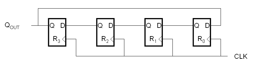
The circuit shown below, commonly known as a "ring register," is a simple linear feedback shift register.
For those that are familiar with circuit diagrams of this kind, the first thing you might notice is that the circuit is drawn backwards from the normal convention, meaning that signals flow from right-to-left instead of from left-to-right. This is done intentionally so that, later on, the contents of the registers will map to the coefficients of polynomial expressions in a fashion that is familiar to us.
For those not familiar with digital registers, each box shown above is known as a D-type Flip Flop (DFF). A DFF has a clock input (shown by the triangle on the bottom input which, technically, only means that the input is edge-sensitive), a D input, and a Q output. There is normally a Qb output as well, which is simply the opposite of whatever the Q output happens to be. Since we will not be using the Qb output, we will not show it. Likewise, we will soon dispense with the clock signal altogether - not because it isn't used, but because its use is well defined and unchanging therefore there is no need to clutter our diagrams, just as we are already not cluttering them with the power supply connections even though the circuit must have them to function at all.
The conceptual operation of a DFF is very simple. At each rising clock edge, whatever value is present at the D input is captured, stored internally, and echoed to the Q output. This value continues to be held, even if the value at the D input changes, until the next rising clock edge. The astute observer might wonder what happens when all of the DFF's are clocked simultaneously since the D input to one DFF is the Q output of another DFF which is, potentially, changing at the same time. The answer is that it takes a finite amount of time for the output of a DFF to respond to a clock pulse and as long as each DFF is finished with its present D input value before any changes due to other DFFs arrive, the circuit will behave correctly. We will assume that this is the case here, but it should be noted that in real circuits these are issues that must be considered.
To be clear on our nomenclature, if we refer to Q2 we mean the Q output of R2, while if we refer to D3 we mean the D input of R3. Since these two signals share the same line in the diagram, they are, in fact, the same signal. Likewise, QOUT, Q3, and D0 all refer to the same signal.
Our simplified diagrams will follow a very simple convention: Each DFF is represented by a box, usually with an identifying label in it. The D input is indicated by a line with an arrow going toward the DFF while the Q output is indicated by a line with an arrow going away from it. The Qb output is unused and omitted. While the clock input is omitted, its use is understood and global (common) to all DFFs in the circuit. By imposing these simplifications, we can draw the circuit above more simply as:
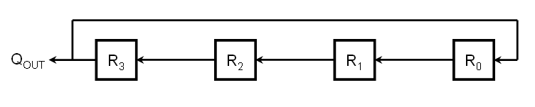
Assume that the contents in the registers are, from left to right, {1,0,1,1}. The contents of the registers and the output of the circuit (QOUT) as we begin clocking it would then be:
| CLK | Contents | QOUT |
| 0 | 1011 | 1 |
| 1 | 0111 | 0 |
| 2 | 1110 | 1 |
| 3 | 1101 | 1 |
| 4 | 1011 | 1 |
As you can see, after four clock cycles, the contents of the shift register have returned to the original state, hence the output of the circuit repeats itself every four clock cycles. With a little consideration, it becomes obvious that we can load the shift register in such a way that it repeats itself in fewer than four clock cycles. For instance, if we load it with {1010} it will repeat with a period of two clock cycles.
But what if we want it to repeat itself in greater than four clock cycles? The circuit, as drawn, can't accomplish this. But notice that we have only one feedback path. Namely, the only register whose next state is directly dependent on the state of one or more registers further down the line is R0. What if we added more feedback paths? As a simple example, let's make the next value of R2 be the exclusive-OR of the overall output, QOUT, and the output of the prior stage, Q1.
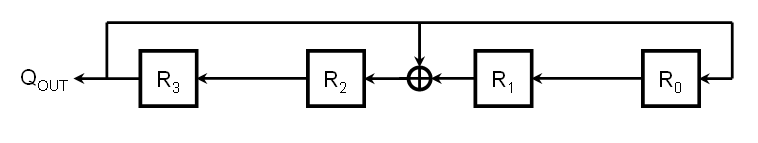
The symbol between R1 and R2 is the boolean algebra operator for exclusive-OR (an addition side within a circle). In an actual circuit, this is simply a two-input XOR gate where the two inputs are QOUT and Q1 while the output is D2.
Working through the states of this circuit yields the following when the initial input is {1011}.
Loop #2
| CLK | Contents | QOUT |
| 0 | 1011 | 1 |
| 1 | 0011 | 0 |
| 2 | 0110 | 0 |
| 3 | 1100 | 1 |
| 4 | 1101 | 1 |
| 5 | 1111 | 1 |
| 6 | 1011 | 1 |
(The reason we are calling this Loop #2 will become apparent in a little bit)
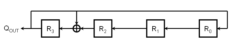
In this case, the system repeats after six clock cycles. So we have established that it is, in fact, possible to get a linear feedback shift register to have a cycle period greater than the number of registers in the circuit. Having established this, we might ask if the repeat period is dictated solely by the circuit configuration. In other words, will we get a period of six clock cycles regardless of what we initially load the registers with? Let's see what happens if we load the machine with {1010) instead.
Loop #1
| CLK | Contents | QOUT |
| 0 | 1010 | 1 |
| 1 | 0001 | 0 |
| 2 | 0010 | 0 |
| 3 | 0100 | 0 |
| 4 | 1000 | 1 |
| 5 | 0101 | 0 |
| 6 | 1010 | 1 |
This also repeats after six clock cycles, which might lead us to conclude that, yes, no matter what we initially load the registers with, this particular circuit configuration will always repeat with a period of six clock cycles. Well, first off, this is highly anecdotal and circumstantial; we don't want to make any strong conclusions yet. So let's consider the following. The first example covered six of the possible sixteen internal states. If we had initialized the machine to any of these six states, we would have been in the same loop, just starting at a different point, thus all of these states are "members" of the same loop. The same is true for the second loop regarding a different set of six of the possible sixteen states. Hence the behavior for twelve of the states is already established leaving only four states to work with.
Loop Membership
| State | Contents | Period | Loop # |
| 0 | 0000 | ? | ? |
| 1 | 0001 | 6 | 1 |
| 2 | 0010 | 6 | 1 |
| 3 | 0011 | 6 | 2 |
| 4 | 0100 | 6 | 1 |
| 5 | 0101 | 6 | 1 |
| 6 | 0110 | 6 | 2 |
| 7 | 0111 | ? | ? |
| 8 | 1000 | 6 | 1 |
| 9 | 1001 | ? | ? |
| 10 | 1010 | 6 | 1 |
| 11 | 1011 | 6 | 2 |
| 12 | 1100 | 6 | 2 |
| 13 | 1101 | 6 | 2 |
| 14 | 1110 | ? | ? |
| 15 | 1111 | 6 | 2 |
Clearly these four states can't form a loop with a period of six clock cycles. So what do they result in? Let's start from the top with {0000}.
Loop #0
| CLK | Contents | QOUT |
| 0 | 0000 | 0 |
| 1 | 0000 | 0 |
What we have gotten is a loop with a period of just a single clock cycle, meaning that it doesn't change at all. For the types of shift register topologies we will be looking at, this will always be the case. Hence we have called this "Loop #0" and will treat it as a "disallowed" state meaning that we must insure that our circuit never enters this state (unless we want our shift register to stall).
The next state that is unaccounted for is {0111}.
Loop #3
| CLK | Contents | QOUT |
| 0 | 0111 | 0 |
| 1 | 1110 | 1 |
| 2 | 0001 | 1 |
| 1 | 0111 | 0 |
This loop has a period of three clock cycles and accounts for all of the remaining internal states.
Instead of tabulating all of the internal states and which loop they belong to again, we will instead tabulate the loops indicating what their period is and give only one of the internal states within that loop. For convenience, we will indicate the internal state that is "smallest" when the bit sequence is interpreted as an integer and we will number the loops in order accordingly as well. We also omit the case when the internal state is all zeros since that behavior is known and constant.
Loop Summary
| Loop # | Seed | Period |
| 1 | 0001 | 6 |
| 2 | 0011 | 6 |
| 3 | 0111 | 3 |
An obvious question that suggests itself is whether it is possible to devise a feedback configuration such that we only obtain a single loop containing all of the non-zero internal states. Such a loop is known as a "maximal length sequence," also known as an m-sequence. Consider the configuration below:
| CLK | Contents | QOUT |
| 0 | 0001 | 0 |
| 1 | 0010 | 0 |
| 2 | 0100 | 0 |
| 3 | 1000 | 1 |
| 4 | 1001 | 1 |
| 5 | 1011 | 1 |
| 6 | 1111 | 1 |
| 7 | 0111 | 0 |
| 8 | 1110 | 1 |
| 9 | 0101 | 0 |
| 10 | 1010 | 1 |
| 11 | 1101 | 1 |
| 12 | 0011 | 0 |
| 13 | 0110 | 0 |
| 14 | 1100 | 1 |
| 15 | 0001 | 0 |
Since this loop cycles through all possible non-zero states, the circuit is a maximal length sequence generator and will generate the same maximal length sequence regardless of which non-zero initial value we give it. The only difference will be where in the sequence the output begins. In other words, the initial value controls the phase of the sequence, but not the sequence itself.
For a number of reasons, we would like to be able to design circuits that produce maximal length sequences. But how do we do this? One obvious answer is to simply try all of the possible circuits, seed each with a non-zero value, and see if which ones generate a maximal length sequence. But how practical is this? First off, what do we mean by "all possible circuits"? Let's restrict our options to allowing the D input of each register to either be the output of the register before it or the exclusive-OR of the output before it and the output of the last stage. This would result in 2n possible configurations, but by examining the first stage, we can see that it makes no sense to do anything but feed the last stage's output directly back into the first stage's input. Hence if we have an n-bit shift register, we have 2(n-1) possible circuits to evaluate. Then, for each circuit, we need to (potentially) clock it through 2n states to determine if it is an m-sequence.
For small shift registers a brute force analysis is doable. For instance, to examine all possible combinations for an eight bit shift register, the maximum number of clock cycles that we would have to work through would be 215, which is only 32,768. Even a 16-bit shift register would only involve, at most, 231 clocks, which is just a bit over two billion. Today's computers could probably exhaust the search space in only a few seconds to a few hours, depending on how well written the code was. But what about a 32-bit shift register? This would involve up to 263 clock cycles and even if the evaluating machine were clocked at 1 GHz, it would take nearly three centuries to complete the task on a single machine. There is no point even discussing how long such a search would take for a 64-bit shift register; for those that are interested, if there were a billion machines working on the problem, each capable of clocking at 1 GHz, it would take approximately 400 times the estimated age of the universe to complete.
Given that modern processors are commonly 64-bit, it is not unreasonable to suspect that 64-bit m-sequence generators are desirable for at least some applications. Hence we need a better way of identifying appropriate circuit configurations. The answer is to exploit the mathematics associated with finite field arithmetic.
From the material on polynomial arithmetic in GF(pn), where p is a prime number and n is a positive integer, we know the following:
In order to give us something concrete to work with and to provide a convenient tie to the material in the previous section, we'll look at GF(24). In this finite field, our symbols are of the form:
A = a3D3 + a2D2 + a1D + a0
Similarly, our modulus polynomial can be represented in the form:
M = D4 + m3D3 + m2D2 + m1D1 + 1
We know that each possible non-zero value of A maps to DK for some particular value of K. Well refer to this value of A as AK. We may or may not know the exact value of K for a given A, but we know that we can generate all of the possible values of AK, and therefore all of the non-zero values of A, by using (pn-1) consecutive values of k starting at K. Right now we are only interested in generating the next value of A in the sequence, namely A(K+1) which maps to D(K+1). However, this can also be written as follows:
A(K+1) = D(K+1) mod M
A(K+1) = ((DK)(D)) mod M
A(K+1) = (AKD) mod M
Therefore, given a particular value of AK, we can express A(K+1) as follows:
AK = a3D3 + a2D2 + a1D + a0
A(K+1) = (a3D4 + a2D3 + a1D2 + a0D) mod M
Next, consider the consequences of the following obvious statement:
M mod M = 0
From this we have:
M mod M = (D4 + m3D3 + m2D2 + m1D1 + 1) mod M = 0
D4 = -(m3D3 + m2D2 + m1D1 + 1)
This means that A(K+1) can be expressed as:
A(K+1) = (a3(-(m3D3 + m2D2 + m1D1 + 1)) + a2D3 + a1D2 + a0D) mod M
Collecting together the terms of the same order, we have:
A(K+1) = ( (a2-a3m3)D3 + (a1-a3m2)D2 + (a0-a3m1)D + (-a3m0) ) mod M
Since it is understood that each coefficient will be reduced modulo-2, we will end up with a polynomial that is a member of our symbol set and hence there is no need to reduce it mod-M.
A(K+1) = (a2-a3m3)D3 + (a1-a3m2)D2 + (a0-a3m1)D + (-a3m0)
Notice that the new value of each coefficient can be written as
a'j = a(j-1) - anmj
This even holds for a'j provided we define a(-1) to be 0, which is not unreasonable. We also know that m0 is always 1.
Notice that the next state of any register is dependent only upon the state of the prior register, the state of the final register, and the value of a specific bit in the modulus polynomial. Furthermore, the relationship between these three inputs is independent of which register is being considered. Therefore we can design a simple combinatorial logic circuit that takes three inputs and produces a single output and insert it before each stage of the shift register as follows:
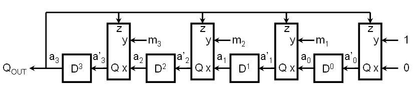
So what must our logic circuit look like? One way to answer this question is by simply generating the necessary truth table and then designing a circuit that implements that truth table. The truth table can be generated by evaluating the next-state equation for all possible inputs.
In terms of the logic circuit inputs and outputs, our next-state equation requires that the logic circuit implement the following function:
Q = (x - zy) mod 2
Let's first evaluate this expression by brute force and then evaluate it using a bit more elegant approach.
| x | y | z | x - zy | Q = (x-xy) mod 2 |
| 0 | 0 | 0 | 0 | 0 |
| 0 | 0 | 1 | 0 | 0 |
| 0 | 1 | 0 | 0 | 0 |
| 0 | 1 | 1 | -1 | 1 |
| 1 | 0 | 0 | 1 | 1 |
| 1 | 0 | 1 | 1 | 1 |
| 1 | 1 | 0 | 1 | 1 |
| 1 | 1 | 1 | 0 | 0 |
Now let's evaluate the expression using a softer touch. We can perform each operation in order and reduce all intermediate results modulo-2 before proceeding. Instead of working with multiplication and subtraction, we will (somewhat arbitrarily, but in order to make a point) choose to work with multiplication, addition, and the additive inverse operations.
Q = (x - zy) mod 2
Q = (x + ( -((zy) mod 2) mod 2) mod 2
So we must define the logic circuits that perform the following three operations:
Q = (-a) mod 2
Q = (a + b) mod 2
Q = (ab) mod 2
It might be tempting to think that the first operation, additive inverse, is going to be the same as logical inversion. However, remember that the definition of the additive inverse of a number is a second number that, when added to the first, results in a value of zero.
| a | -a | Q = (-a) mod 2 |
| 0 | 0 | 0 |
| 1 | -1 | 1 |
The additive inverse of 0 is therefore obviously zero. The additive inverse of 1 is, perhaps somewhat surprisingly, 1 since 1+1 is equal to 2 which reduces to 0 modulo-2. Therefore every number, all two of them, in GF(2) is its own additive inverse. A direct consequence of this is that, in GF(2n), there is no distinction between addition and subtraction.
Turning our attention to addition in a mod-2 world, we have the following truth table that is easily recognized as that of an XOR gate.
| a | b | a + b | Q = (a + b) mod 2 |
| 0 | 0 | 0 | 0 |
| 0 | 1 | 1 | 1 |
| 1 | 0 | 1 | 1 |
| 1 | 1 | 2 | 0 |
Finally, the truth table for multiplication in a mod-2 world reveals it to be nothing more than a logical AND operation.
| a | b | ab | Q = (ab) mod 2 |
| 0 | 0 | 0 | 0 |
| 0 | 1 | 0 | 0 |
| 1 | 0 | 0 | 0 |
| 1 | 1 | 1 | 1 |
Regardless of which approach we used, the ultimate result is that our modulo-2 arithmetic expression reduces to the following boolean expression:
Q = (x) XOR (y AND z)
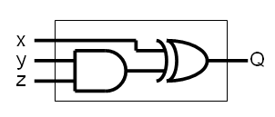
While this logic is easily implemented in either hardware or software, there is yet another simplification we can make if we are working with a fixed modulus polynomial. The key to seeing this simplification is to consider what the circuit reduces to if y (corresponding to mj) is either a fixed 0 or a fixed 1. If y is a fixed 0, then the output of the AND gate is always 0 and, as a consequence, the output of the XOR gate is always equal to Q; the entire circuit can be replaced with a straight wire between x and Q, which corresponds to a simple shift of the previous stage's output into the next stage. On the other hand, if y is a fixed 1, then the output of the AND gate is always equal to z and, as a consequence, the output of the XOR reduces to the exclusive-OR of x and z, which corresponds to the XOR of the previous stage's output with the output of the final stage.
With this in mind, the maximal length sequence generator we found in a prior section can be seen to map to the modulus polynomial coefficients as follows:
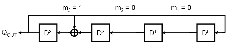
Since we know that mn and m0 are both always equal to 1, this generator implements the modulus polynomial 11001 which, expanded, is
M = D4 + D3 + 1
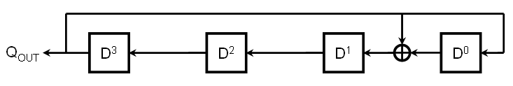
Another primitive polynomial for GF(24) is M = D4 + D + 1. This results in the following shift register configuration:
| CLK | Contents | QOUT |
| 0 | 0001 | 0 |
| 1 | 0010 | 0 |
| 2 | 0100 | 0 |
| 3 | 1000 | 1 |
| 4 | 0011 | 0 |
| 5 | 0110 | 0 |
| 6 | 1100 | 1 |
| 7 | 1011 | 1 |
| 8 | 0101 | 0 |
| 9 | 1010 | 1 |
| 10 | 0111 | 0 |
| 11 | 1110 | 1 |
| 12 | 1111 | 1 |
| 13 | 1101 | 1 |
| 14 | 1001 | 1 |
| 15 | 0001 | 0 |
As expected, this loop cycles through all possible non-zero states and is therefore a maximal length sequence generator.
You might be wondering what other primitive polynomials are available. The answer is that these are the only two primitive polynomials for GF(24). The number of primitive polynomials for a particular length shift register is given by
N = ![]() (2n
- 1) / n
(2n
- 1) / n
where ![]() (n)
is Euler's Totient Function. The
following table shows how many primitive polynomials exist for each length shift
register up to 16-bits and then also for 24-bits and 32-bits.
(n)
is Euler's Totient Function. The
following table shows how many primitive polynomials exist for each length shift
register up to 16-bits and then also for 24-bits and 32-bits.
| n | 2n-1 | Factorization | N | Example M |
| 1 | 1 | (1) | 1 | D+1 |
| 2 | 3 | (3) | 1 | D2 + D + 1 |
| 3 | 7 | (7) | 2 | D3 + D2 + 1, D3 + D + 1 |
| 4 | 15 | (3)(5) | 2 | D4 + D3 + 1, D4 + D + 1 |
| 5 | 31 | (31) | 6 | D5 + D2 + 1, D5 + D4 + D3 + D2 + 1 |
| 6 | 63 | (7)(9) | 8 | D6 + D1 + 1, D6 + D5 + D3 + D2 + 1 |
| 7 | 127 | (127) | 18 | D7 + D + 1, D7 + D6 + D5 + D4 + D3 + D2 + 1 |
| 8 | 255 | (3)(5)(17) | 16 | D8 + D4 + D3 + D2 + 1, D8 + D7 + D6 + D5 + D2 + D + 1 |
| 9 | 511 | (7)(73) | 56 | |
| 10 | 1023 | (3)(11)(31) | 60 | |
| 11 | 2047 | (23)(89) | 176 | |
| 12 | 4095 | (32)(5)(7)(13) | 144 | |
| 13 | 8191 | (8191) | 630 | |
| 14 | 16383 | (3)(43)(127) | 756 | |
| 15 | 32767 | (7)(31)(151) | 1800 | |
| 16 | 65535 | (3)(5)(17)(257) | 2048 | D16 + D5 + D3 + D2 + 1, D16 + D15 + D13 + D4 + 1 |
| 24 | 16777215 | (32)(5)(7)(13)(17)(241) | 276480 | D24 + D4 + D3 + D + 1 |
| 25 | 33554431 | (31)(601)(1801) | 1296000 | |
| 32 | 4294967295 | (3)(5)(17)(257)(65537) | 67108864 | D32 + D22 + D2 + D + 1 |
Let's develop a program that allows us to define a generic linear feedback shift register having a variable number of bits with a user-defined polynomial and seed value. The program will then run the machine until it repeats itself and report the cycle length.
For convenience, we will stipulate a maximum machine length of 32-bits, which maps very conveniently into an unsigned long integer in most C implementations.
The implementation is quite straightforward. Recall from the previous section that the generic shift register is the following:
Also recall that the basic relationship we need to implement is
a'j = a(j-1) - anmj
Using bitwise operations, this can almost be implemented directly. With two minor tweaks, it can be implemented directly. First, we will test the last bit of the shift register and set the feedback value to a field of either all 0's or all 1's accordingly. We will then shift the present value to the left one position and then perform the indicated bitwise operations. The resulting code is as follows:
#include <stdio.h>


int main(void)

{

    unsigned long int State, Poly, Seed;

    unsigned long int Q0, Q1, Qf, Qtest, Mask, temp;

    unsigned long int length;

    int bits;


    /* Values for this run */

    Poly = 0x02400001L;

    Seed = 0x00000001L;


    /* Set Static Masks */

    Q0 = 0;

    Q1 = ~Q0;


    /* Determine length of LSFR */

    for (temp = Poly>>1, bits = 0; temp; temp>>=1)

    {

        bits++;

    }


    /* Generate Output and LFSR masks */

    for (temp = 1, Qtest = 1, Mask = 1; temp < bits; temp++)

    {

        Qtest <<= 1;

        Mask = (Mask << 1) + 1;

    }


    printf("Bits: %2i Poly: 0x%08lX Seed: 0x%08lX\n", bits, Poly,
Seed);

    printf("Maximal Length Sequence:... %10lu cycles.\n", Mask);


    /* Run machine */

    length = 0;

    State = Seed;

    do

    {

        length++;

        Qf = (Qtest&State)? Q1 : Q0;

        State = Mask & ((State << 1) ^ (Qf &
Poly));

    } while (State != Seed);


    /* Output Results */

    printf("Actual Sequence Length:.... %10lu cycles.\n",
length);


    return 0;

}
In the above example, the polynomial and the seed are hard coded for convenience. The particular polynomial used is a primitive polynomial for a 25-bit shift register. The static masks Q0 and Q1 are simply masks that are all zeros or all ones, respectively. These are used to feedback the appropriate value of the output bit to all of the registers.
The number of bits in the LFSR is determined by the polynomial; in particular, by the position of the leftmost 1 in the polynomial. The loop simply makes a copy of the polynomial and counts how many times it must be shifted to the right until only zero bits remain. Notice that this trick means that the polynomial value must have all of the coefficients in it and therefore the largest machine we can actually run is a 31-bit machine. If we specify the length of the machine separately, we can run a 32-bit machine because the high order bit is not actually used for anything meaningful.
Since the output bit is embedded in a 32-bit State string and since there are possibly unused bits at the left end of the State string, a couple of masks are generated to deal with this. The first mask, Qtest, needs to have a 1 only in the position that corresponds to the LFSR output bit. The second mask, Mask, needs to have 1's in all of the positions that are actually in use. Both of these masks can be generated by starting a single 1 bit at the right end of a mask and left-shifting it a number of times determined by the length of the LFSR and backfilling the Mask mask on the right.